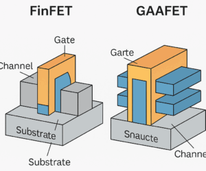
Shrinking process nodes has never been a simple matter of scaling dimensions. As devices move beyond the 3nm threshold, traditional transistor architectures struggle to maintain control over leakage, variability, and power efficiency. This transition marks a decisive shift toward Gate-All-Around Field-Effect Transistors, commonly referred to as GAAFETs, which redefine how current flows and how gates interact with channels at nanoscale levels.
Design ecosystems are evolving alongside these structural changes, requiring deep expertise in device physics, modeling, and system-level integration. Organizations operating as a VLSI design company are now expected to translate these architectural shifts into manufacturable silicon while aligning with advanced-node constraints and verification requirements.
Understanding the Shift from FinFET to GAAFET
FinFET technology introduced multi-gate control that significantly improved electrostatics over planar devices. However, as nodes approach and go beyond 3nm, fin structures face limitations in suppressing leakage and maintaining consistent channel control.
GAAFET architectures address these constraints by surrounding the channel entirely with a gate structure. This enables superior electrostatic control and reduces short-channel effects, allowing continued scaling without severe performance degradation.
Device Architecture and Electrostatic Advantages
GAAFETs replace fin structures with nanosheets or nanowires stacked vertically. This configuration allows designers to tune channel width by adjusting sheet dimensions, offering flexibility without increasing silicon area.
Enhanced gate control improves threshold stability and reduces leakage currents. As a result, switching efficiency improves while standby power decreases, which is essential for modern processors and power-sensitive applications.
Impact on Power Silicon Design
Power silicon design is undergoing a structural transformation with GAAFET adoption. Reduced leakage and improved gate modulation directly impact energy efficiency, particularly in high-density and high-performance systems.
Engineers must rethink voltage scaling strategies, power grids, and thermal behavior. These changes demand a co-optimized design approach where device physics and system architecture are aligned for optimal performance.
Challenges in Manufacturing and Process Integration
Fabricating GAAFETs introduces significant complexity due to the need for precise nanosheet stacking and uniform channel formation. Variability at such scales can affect both yield and reliability.
Advanced lithography and material deposition processes must operate within tighter tolerances. This increases dependency on design-manufacturing collaboration, especially in advanced-node environments where margins are minimal.
Variability Control in Nanosheet Structures
Maintaining consistency in nanosheet thickness and spacing is critical. Even slight deviations can introduce variability in electrical characteristics across devices.
Accurate modeling and simulation help mitigate these risks. Early-stage prediction allows engineers to adjust process parameters and improve yield outcomes.
Thermal Management Considerations
Higher device density results in localized heat concentration. Even with improved efficiency, thermal hotspots remain a concern in advanced nodes.
Thermal-aware design practices ensure long-term reliability. Efficient heat dissipation strategies are essential to maintain stable operation under continuous workloads.
Advanced Lithography Requirements
Extreme ultraviolet lithography enables patterning at nanoscale precision required for GAAFET fabrication. However, it demands strict alignment between design rules and manufacturing capabilities.
Any deviation can introduce defects or performance inconsistencies. This makes integration between design teams and fabrication processes increasingly critical.
Material Engineering Complexity
Material selection plays a vital role in GAAFET performance. Gate dielectrics, channel materials, and interfaces must be optimized for conductivity and durability.
Continuous innovation in materials is necessary to meet performance targets. Engineers must balance electrical efficiency with compatibility across fabrication steps.
Design Flow Evolution for Advanced Nodes
Design flows must evolve to accommodate the complexity introduced by GAAFET architectures. Traditional methodologies may not capture the nuances of multi-gate structures and nanoscale variability.
Advanced simulation, parasitic extraction, and timing analysis are essential to ensure accuracy. These improvements help designers predict behavior under real-world operating conditions.
- Advanced-node design now requires tighter integration between front-end and back-end flows
- Timing closure becomes more complex due to new switching characteristics
- Power modeling must reflect reduced leakage and dynamic behavior
Role of System-Level Optimization
Device-level advancements alone cannot guarantee performance improvements. System-level optimization is necessary to fully leverage GAAFET capabilities.
Workload-aware design, memory hierarchy optimization, and interconnect efficiency play a crucial role. These elements ensure that transistor-level gains translate into system-wide benefits.
- Efficient data movement reduces unnecessary switching activity
- Memory architecture must align with faster transistor speeds
- Interconnect design influences latency and throughput
Integration with Modern Design Methodologies
Modern semiconductor development depends on structured design flows that integrate verification, validation, and implementation. GAAFET adoption amplifies the need for precision at every stage.
One critical layer is RTL design, where system intent is translated into hardware description. Strong front-end design practices ensure alignment with downstream processes such as physical implementation and test integration. Tessolve, for instance, offers end-to-end VLSI services including RTL, DFT, and physical design, enabling smoother transitions from specification to silicon.
- Early verification reduces costly redesign cycles
- Scalable architectures adapt better to new nodes
- Cross-functional alignment improves overall design quality
Industry Implications and Competitive Landscape
The move to GAAFET technology is reshaping the semiconductor ecosystem. Companies that successfully adopt these architectures gain advantages in efficiency, scalability, and performance.
Investment in R&D, advanced packaging, and system integration is accelerating. Industry leaders are focusing on end-to-end capabilities, combining design, testing, and product engineering to remain competitive.
- Strong ecosystem partnerships are becoming essential
- End-to-end engineering capabilities are gaining importance
- Innovation speed determines market leadership
Final Thoughts
What does it take to lead in an era where transistor architecture itself is being reinvented? GAAFETs are not just a continuation of scaling but a fundamental redesign of how silicon behaves, demanding expertise across design, validation, and manufacturing.
In this evolving landscape, Tessolve stands out as an end-to-end semiconductor engineering partner, offering capabilities from chip design and verification to test engineering, PCB design, and system-level solutions. With experience spanning pre-silicon and post-silicon stages and serving a majority of top semiconductor firms globally, it enables companies to move from concept to production with greater confidence.
As the race toward advanced nodes intensifies, the ability to integrate design precision with manufacturing readiness will define the biggest semiconductor company in the years ahead.